Microsystems Test Facility
The Microsystems Test Facility offer a wide range of Optical and Electrical test capabilities for wafer, frame, die, or module level testing. We develop test systems for all stages of product maturity - spanning early-stage experiments, to harsh-environment reliability, and production-scale tests under a ISO-9001 Quality Management System. Our expert team of Design, Test, and System Engineers customizes test solutions to meet technology and product requirements, and has decades of combined deep experience in semiconductor & microsystem electronics. We transition the systems to production-scale either internally or with preferred contract manufacturers, depending on the customer’s desired outcome.
Electrical Testing
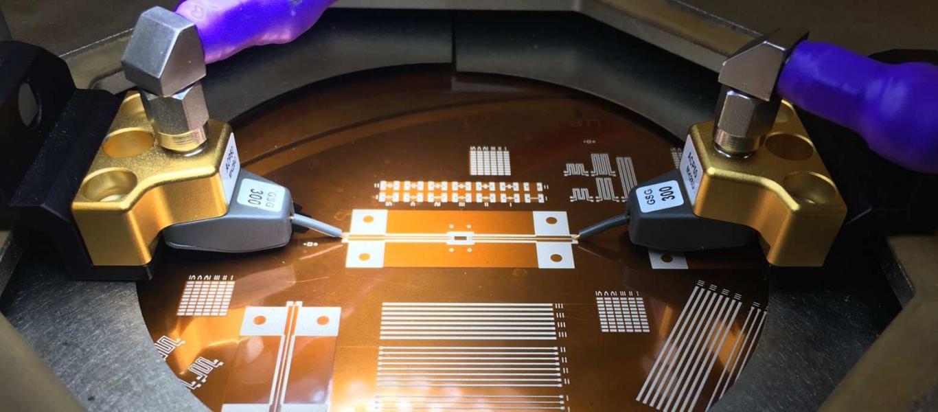
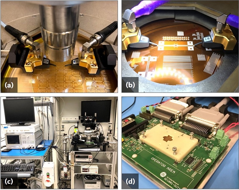
Wafer/Frame Probing
- Fully automated, semi-automated, and manual probers available (-55°C to 620°C capable)
- Easily configurable with stack-and-rack electrical test equipment, enabling quick development & results
- Customizable connectors & fixturing
- Hardware capability ranging from high-power (5KV/350A) to low-noise measurements (1E-14 Amp/Farad/Henry)
- High-density switch matrices for multi-point measurement routines
RF Testing
- RF probe station w/ variety of probe styles & pitches
- 50GHz capable hardware w/ 70GHz-capable VNA, hot & cold chuck for -60°C to 200°C RF probing
- Time-domain reflectometry (TDR) for RF circuit analysis - down to the component level
- Load-pull measurement system for RF circuit impedance characterization
- Non-invasive test for characterization of materials’ dielectric constant & loss tangent at RF frequencies (up to 10GHz)
Vacuum Probing
- Probe stations capable of electrical test of partial or full wafers (up to 2” diameter)
- Sample temperatures range of -253°C to 400°C, vacuum level down to 10e-5 torr
- External DC Bias and Network Analyzer to 70GHz
- Advanced frequency response test capability including automated data acquisition and lock-in amplifier system
- Chamber backfill capability for testing in research-grade gas environments
Benchtop Testing
- High-temperature in-situ electrical test chambers up to 300°C
- Harsh-environment chambers for HAST testing (humidity chamber, thermal shock, etc.)
- Hermetic package leak rate tester (non-destructive, helium bomb & sniff)
- Chip carrier packaging processes w/ compatible socket testers for quick device building
- Custom test fixture design to accommodate unique device designs (ex. pogo-pin testers)
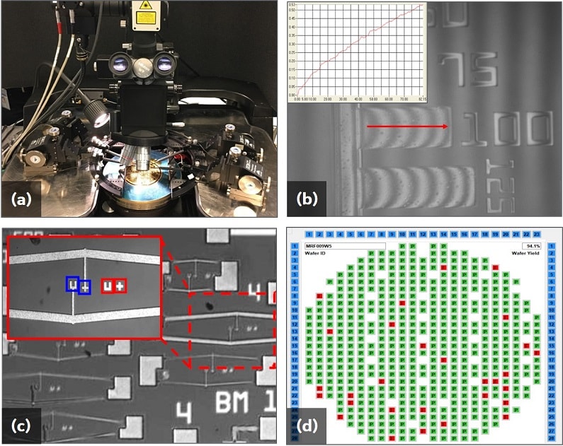
Optical Testing
Laser-Doppler Vibrometer (LDV)
- Out-of-plane vibration velocity measurements for dynamic characterization of actuated structures
- < 3um/sec resolution , < 1nm displacement resolution (calculated)
- 10MHz max. oscillation frequency measurable
- LDV system integrated onto automated wafer prober, enabling multiple-point scanning for 3D profile animations
- 5um diameter min. measurement spot size for single-point measurements
Interferometry
- Long working distance phase-shifting interferometer for static out-of-plane surface profile measurements
- < 10nm absolute deflection resolution, with automatic background/substrate tilt compensation
- Integrated with electrical probes & mechanical force probes (piezo-pusher)
- Strip heater for up to 500°C in-situ testing, rapid heating & cool-down
- Configurable optical paths for measurements through opaque encapsulating materials (ex. thin film on glass)
Optical In-Plane Displacement Measurements
- Utilizing MEMSuite software’s sub-pixel image analysis, pattern matching, and auto-focusing capabilities
- 1nm position/displacement measurement resolution
- Bent-beam structure measurements of wafer residual stress (“bow-tie” design references available)
- Stroboscopic measurement for high-speed displacement measurements
- Implemented in automated test systems to ensure highly-accurate & repeatable data
Automated Image Capture & Visual Inspection
- Pattern-matching for guided image capture, visual inspection, & robust auto-focusing
- Multi-FOV stitching to create high-magnification large field of view image
- Capture entire slides, wafers, material samples, etc.
- Temperature control integration
- Light source intensity measurements (ex. LED characterization)


GE leverages its multidisciplinary core capabilities to design and develop advanced solutions to complex, challenging problems.
Learn More-
0Global Research Centers
-
0k+Square Feet of Laboratory Space
-
0+Staff Scientist, Engineers & Technicians
-
0+PhDs