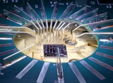
Cleanroom Facility
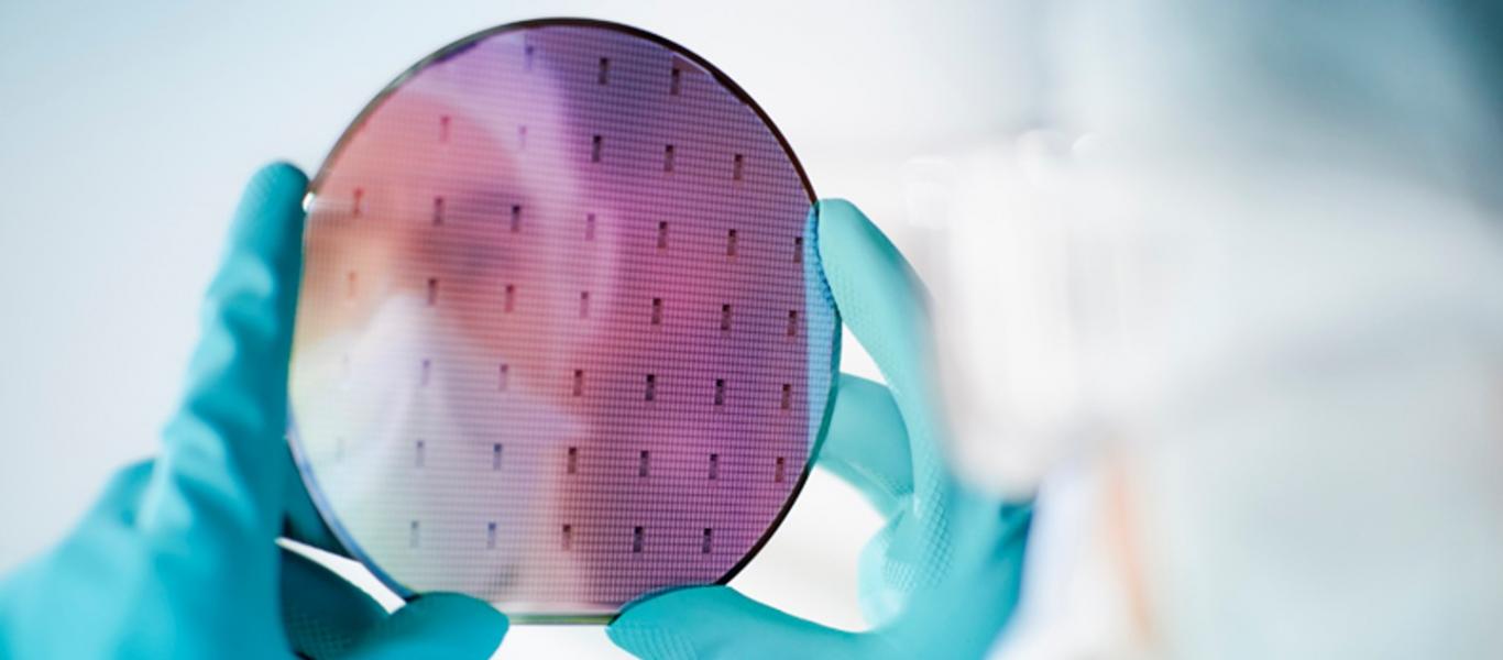
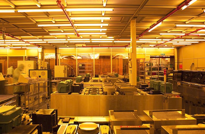
The Electronics cleanroom is a 28,000 sq. ft. of Class 100/1000 (ISO 9000 certified) R&D facility containing more than 200 pieces of semiconductor processing equipment in unit step areas including oxidation, anneal and LPCVD furnace processing; dielectric PECVD deposition; metal deposition (sputter, electroplate, electroless, ebeam, thermal evaporation); dry etching; laser drilling and patterning; wafer dicing; wet processing; metrology; and photolithography. These areas are staffed with experienced unit step leaders, engineers, and processing technicians who have worked in that area over many years. These teams maintain equipment and process control, establish new processes, troubleshooting existing processes, and acquire new equipment for expansion and next generation devices.
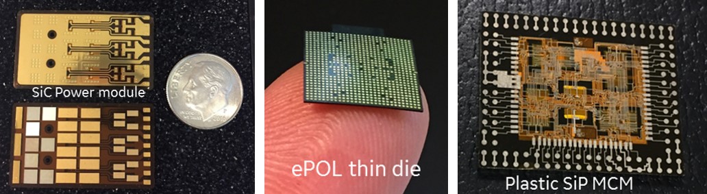
Products and services range from off the shelf systems or devices to full fabrication flows, process modules, or individual steps. We bring technology from R&D through low-volume production and transfer technology to high-volume manufacturing.


GE leverages its multidisciplinary core capabilities to design and develop advanced solutions to complex, challenging problems.
Learn More-
0Global Research Centers
-
0k+Square Feet of Laboratory Space
-
0+Staff Scientist, Engineers & Technicians
-
0+PhDs